- 您现在的位置:买卖IC网 > Sheet目录472 > MAX2370EVKIT (Maxim Integrated)EVAL KIT MAX2370
�� �
�
�Complete� 450MHz� Quadrature� Transmitter�
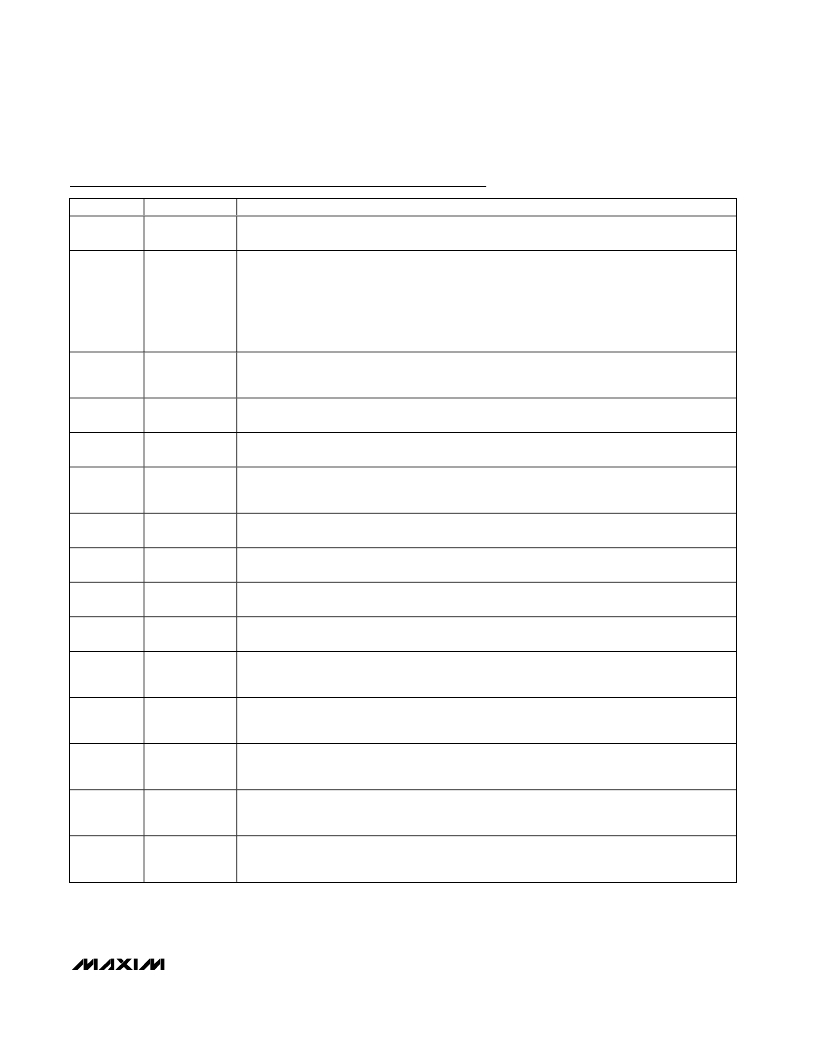
�Pin� Description� (continued)�
�PIN�
�13,� 14,� 15�
�NAME�
�CLK,� DI,� CS�
�FUNCTION�
�CMOS� Inputs� from� the� 3-Wire� Serial� Bus� (SPI/QSPI/MICROWIRE� Compatible).� A� small� RC�
�lowpass� filter� on� each� of� these� pins� can� be� used� to� reduce� noise� on� these� lines.�
�Differential� IF� Outputs.� This� port� is� active� when� IF_SEL� is� LOW� and� supports� both� FM� and� CDMA�
�modes.� IFOUT+� and� IFOUT-� must� be� inductively� pulled� up� to� V� CC� and� differentially� loaded� with�
�typically� 560� ?� .� A� 400� ?� differential� IF� bandpass� filter� is� connected� between� this� port� and� IFIN+/-.�
�18,� 19�
�IFOUT-,� IFOUT+� The� pullup� inductors� can� be� part� of� the� filter� structure.� The� differential� output� impedance� of� this�
�port� is� nominally� 400� ?� ,� including� the� 560� ?� external� differential� resistor.� Keep� the� transmission�
�lines� from� these� pins� as� short� as� possible� to� minimize� the� unintentional� pickup� of� spurious� signals�
�and� noise.�
�RF� and� IF� Gain-Control� Analog� Input.� Accepts� input� voltages� from� 0.5V� (minimum� gain)� to� 2.5V�
�20�
�21�
�22�
�23,� 24�
�25,� 26�
�27�
�28�
�29�
�30,� 31�
�36�
�37�
�38�
�39�
�GC�
�V� CC�
�V� CC�
�Q+,� Q-�
�I+,� I-�
�SHDN�
�V� CC�
�IFLO�
�TANK-,� TANK+�
�REF�
�V� CCIFCP�
�IFCP�
�V� CC�
�(maximum� gain).� When� not� driven,� GC� is� internally� biased� to� typically� 1.5V.� RC� lowpass� filter� the�
�voltage� applied� to� this� pin� to� remove� DAC� noise� or� PDM� clock� spurs.�
�Power� Supply� for� the� IF� VGA.� Bypass� to� PC� board� ground� with� a� 0.1μF� capacitor� placed� as� close�
�to� the� pin� as� possible.� Do� not� share� capacitor� ground� vias� with� other� ground� connections.�
�Power� Supply� for� the� I/Q� Modulator.� Bypass� to� PC� board� ground� with� a� 0.1μF� capacitor� placed� as�
�close� to� the� pin� as� possible.� Do� not� share� capacitor� ground� vias� with� other� ground� connections.�
�Differential� Q-Channel� Baseband� Inputs� to� the� Modulator.� Q+� and� Q-� connect� directly� to� the�
�bases� of� a� differential� pair� and� require� a� typical� 1.35V� to� (V� CC� -� 1.5V)� external� common-mode� bias�
�voltage.�
�Differential� I-Channel� Baseband� Inputs� to� the� Modulator.� I+� and� I-� connect� directly� to� the� bases� of�
�a� differential� pair� and� require� a� typical� 1.35V� to� (V� CC� -� 1.5V)� external� common-mode� bias� voltage.�
�Digital� Input.� Drive� LOW� to� shut� down� the� entire� IC,� drive� high� for� normal� operation.� A� small� RC�
�lowpass� filter� can� be� used� to� filter� digital� noise.�
�Power� Supply� for� the� VCO� Section.� Bypass� to� PC� board� ground� with� a� 0.1μF� capacitor� placed� as�
�close� to� the� pin� as� possible.� Do� not� share� capacitor� ground� vias� with� other� ground� connections.�
�IF� LO� Output.� Provides� access� to� the� IF� VCO� output� and� can� be� used� to� drive� an� external� PLL.� It� can�
�be� disabled� by� logic-low� on� the� BUF_EN� control� bit.� IFLO� is� internally� biased� to� typically� 1.5V.�
�Differential� Tank� Connections� for� the� IF� VCO.� TANK+� and� TANK-� are� internally� biased� to�
�approximately� 1.6V� and� must� be� AC-coupled� to� the� external� tank� (can� be� DC-coupled� if� tank� does�
�not� sink� or� source� current).�
�Reference� Frequency� Input.� REF� is� internally� biased� to� approximately� 1.0V� and� must� be� AC-�
�coupled� to� the� reference� source.� This� is� a� high-impedance� port� and� must� be� externally� terminated�
�in� the� desired� impedance.�
�Power� Supply� for� the� IF� Charge� Pump.� This� supply� can� be� different� from� the� system� V� CC� .� Bypass�
�to� PC� board� ground� with� a� minimum� 0.1μF� capacitor� placed� as� close� to� the� pin� as� possible.� Do�
�not� share� capacitor� ground� vias� with� other� ground� connections.�
�High-Impedance� IF� Charge-Pump� Output.� Connect� to� the� tune� input� of� the� IF� VCO� through� the� IF�
�PLL� loop� filter.� Keep� the� connection� from� IFCP� to� the� tune� input� as� short� as� possible� to� prevent�
�spurious� pickup.�
�Power� Supply� for� Digital� Circuitry.� Bypass� to� PC� board� ground� with� a� minimum� 0.1μF� capacitor�
�placed� as� close� to� the� pin� as� possible.� Do� not� share� capacitor� ground� vias� with� other� ground�
�connections.�
�_______________________________________________________________________________________�
�7�
�发布紧急采购,3分钟左右您将得到回复。
相关PDF资料
MAX2373EVKIT
EVAL KIT MAX2371, MAX2373
MAX2388EGC+
IC LNA/MIXER W-CDMA 12QFN
MAX2392ETI+T
IC RECEIVERS ZERO-IF 28TQFN-EP
MAX2395ETI+T
IC MOD WCDMA W/DRIVER 28-TQFN
MAX2410EVKIT
EVAL KIT MAX2410
MAX2411AEEI+
IC UP/DOWNCONVERTER 28-QSOP
MAX2510EVKIT-SO
EVAL KIT MAX2510
MAX2511EVKIT
EVAL KIT MAX2511
相关代理商/技术参数
MAX2371EGC
功能描述:射频放大器 RoHS:否 制造商:Skyworks Solutions, Inc. 类型:Low Noise Amplifier 工作频率:2.3 GHz to 2.8 GHz P1dB:18.5 dBm 输出截获点:37.5 dBm 功率增益类型:32 dB 噪声系数:0.85 dB 工作电源电压:5 V 电源电流:125 mA 测试频率:2.6 GHz 最大工作温度:+ 85 C 安装风格:SMD/SMT 封装 / 箱体:QFN-16 封装:Reel
MAX2371EGC+
功能描述:射频放大器 LNAs w/Step Attenuator & VGA RoHS:否 制造商:Skyworks Solutions, Inc. 类型:Low Noise Amplifier 工作频率:2.3 GHz to 2.8 GHz P1dB:18.5 dBm 输出截获点:37.5 dBm 功率增益类型:32 dB 噪声系数:0.85 dB 工作电源电压:5 V 电源电流:125 mA 测试频率:2.6 GHz 最大工作温度:+ 85 C 安装风格:SMD/SMT 封装 / 箱体:QFN-16 封装:Reel
MAX2371EGC+T
功能描述:射频放大器 LNAs w/Step Attenuator & VGA RoHS:否 制造商:Skyworks Solutions, Inc. 类型:Low Noise Amplifier 工作频率:2.3 GHz to 2.8 GHz P1dB:18.5 dBm 输出截获点:37.5 dBm 功率增益类型:32 dB 噪声系数:0.85 dB 工作电源电压:5 V 电源电流:125 mA 测试频率:2.6 GHz 最大工作温度:+ 85 C 安装风格:SMD/SMT 封装 / 箱体:QFN-16 封装:Reel
MAX2371EGC-T
功能描述:射频放大器 RoHS:否 制造商:Skyworks Solutions, Inc. 类型:Low Noise Amplifier 工作频率:2.3 GHz to 2.8 GHz P1dB:18.5 dBm 输出截获点:37.5 dBm 功率增益类型:32 dB 噪声系数:0.85 dB 工作电源电压:5 V 电源电流:125 mA 测试频率:2.6 GHz 最大工作温度:+ 85 C 安装风格:SMD/SMT 封装 / 箱体:QFN-16 封装:Reel
MAX2371ETC+
功能描述:射频放大器 LNAs w/Step Attenuator & VGA RoHS:否 制造商:Skyworks Solutions, Inc. 类型:Low Noise Amplifier 工作频率:2.3 GHz to 2.8 GHz P1dB:18.5 dBm 输出截获点:37.5 dBm 功率增益类型:32 dB 噪声系数:0.85 dB 工作电源电压:5 V 电源电流:125 mA 测试频率:2.6 GHz 最大工作温度:+ 85 C 安装风格:SMD/SMT 封装 / 箱体:QFN-16 封装:Reel
MAX2371ETC+T
功能描述:射频放大器 LNAs w/Step Attenuator & VGA RoHS:否 制造商:Skyworks Solutions, Inc. 类型:Low Noise Amplifier 工作频率:2.3 GHz to 2.8 GHz P1dB:18.5 dBm 输出截获点:37.5 dBm 功率增益类型:32 dB 噪声系数:0.85 dB 工作电源电压:5 V 电源电流:125 mA 测试频率:2.6 GHz 最大工作温度:+ 85 C 安装风格:SMD/SMT 封装 / 箱体:QFN-16 封装:Reel
MAX2371EVKIT#
功能描述:射频开发工具 MAX2371/73 Eval Kit RoHS:否 制造商:Taiyo Yuden 产品:Wireless Modules 类型:Wireless Audio 工具用于评估:WYSAAVDX7 频率: 工作电源电压:3.4 V to 5.5 V
MAX2373E/D-B0A
功能描述:射频放大器 DICE SALES DICE RoHS:否 制造商:Skyworks Solutions, Inc. 类型:Low Noise Amplifier 工作频率:2.3 GHz to 2.8 GHz P1dB:18.5 dBm 输出截获点:37.5 dBm 功率增益类型:32 dB 噪声系数:0.85 dB 工作电源电压:5 V 电源电流:125 mA 测试频率:2.6 GHz 最大工作温度:+ 85 C 安装风格:SMD/SMT 封装 / 箱体:QFN-16 封装:Reel